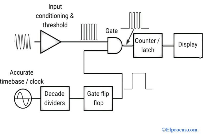
25+ digital frequency counter block diagram
SourceLine Regulation In the block diagram the input line voltage has a nominal value of 230 Volts but in practice here are considerable variations in ac supply mains voltage. We review the recent.
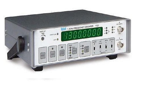
Frequency Counter Block Diagram Circuit Types And Its Applications
Other applications of memristive devices include data encryption 13 14 and radio-frequency RF operations for mobile communications 15 16.
. Proj 25 Smart Antenna Array Using Adaptive Beam forming. Proj 28 Method to Extract Roads from Satellite Images. 16 MHz Internal Oscillator Block.
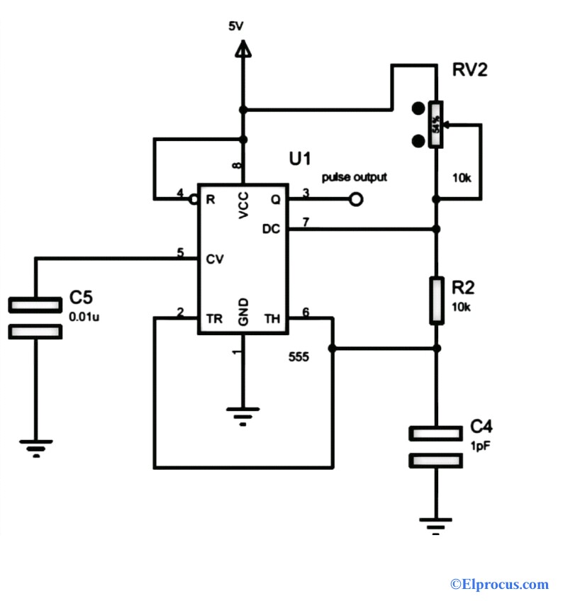
Niknejad PLLs and Frequency Synthesis. P025 is a GPIO digital. Refer Block Diagram of 555 timer IC given above.
Non-linear block that simply acts like a counter. The block diagram down below indicates how a Counter Type ADC works Counter Type ADC Block Diagram Integrating Dual-Slope ADC An integrating ADC dual-slope ADC applies the analog input voltage to the input of an integrator and allows the voltage to ramp for a fixed time period the run-up period. 12 Block diagram The following figure shows a top-level block diagram of the MPC5777C.
Proj 26 Implementation of Butterworth Chebyshev I and Elliptic Filter for Speech Analysis. For the circuit shown the clock frequency is f0 and the duty cycle is 25. Proj 27 Simulator for Autonomous Mobile Robots.
So lets now settle for 256 levels sample points in each cycle of the. TRACEPKT2 is a trace packet bit-2 standard inputoutput port by the inner pull-up. Power Supply and Clock Frequency.
March 2022 DS5319 Rev 18 1116 STM32F103x8 STM32F103xB Medium-density performance line Arm-based 32-bit MCU with 64 or 128 KB Flash USB CAN 7 timers 2 ADCs 9 com. Lets assume its desired to get a sawtooth waveform swinging between 0-5v frequency of 10 Hz. In other words we can say that an electronic device converts the signal of 0 and 1 Binary into the analog form.
- Factory calibrated to 1 typical - Software selectable frequency range from 16 MHz to 31 kHz 31 kHz Low-Power Internal Oscillator Three External Clock modes up to 20 MHz Special Microcontroller Features. For N input edges only one output edge occurs. Here the integer part is 58 and fractional part is 025.
In most applications the control input is not used so that the control voltage equals 23 V CC. Since this ac supply mains voltage is the input to the ordinary power supply the filtered output of the bridge rectifier is almost directly proportional to the ac. AEC-Q100 Grade 1 Qualification is only offered for VQFN with wettable flanks and TQFP devices.
- 18V to 36V PIC16LF15089 - 23V to 55V PIC16F15089. For the signal at the Q output of the Flip-F. IO Pins up to 17 25 25 17 25 ContactLead Pitch 05 mm 05 mm 08 mm 065 mm 04 mm Dimensions 4x4x09 mm 5x5x1 mm 5x5x09 mm2 7x7x1 mm 82x53x20 mm 279x279x0482 mm Notes.
Digital Circuits - Quick Guide If base or radix of a number system is â râ then the numbers present in that number system are ranging from zero to r-1. Configurable as Six Single-Ended Six Dual-Edge Symmetric or Three Dual-Edge Asymmetric Outputs. The internal resistors act as a voltage divider network providing 23Vcc at the non-inverting terminal of the upper comparator and 13Vcc at the inverting terminal of the lower comparator.
The block diagram of 1x16 De-Multiplexer using lower order Multiplexers is shown in the. P118 is a GPIO digital pin. This is information on a product in full production.
RESET IN When the signal on this pin is low0 the program-counter is set to zero. Powering the AM335x AM437x and. The purpose of the block diagram is to show the general interconnection of functional modules through the crossbar switch.
Proj 24 Orthogonal Frequency Division MultiplexingOFDM Signaling. The IMC approach can expend much less power than digital computation of the same operations and could have applications in areas such as robotics and Internet of Things IoT. Interrupts in 8085 microprocessor.
Operating Voltage Range. The contains the subsystems shown in the Functional Block Diagram and a brief description of each follows. Timing diagram of MOV Instruction in Microprocessor.
Dedicated 16-Bit Time-Base Counter With Time and Frequency Controls. But in terms of phase its a linear block F Div F VCO N Div Z t 1 F Divd Z t 1 F VCO N d 1 N Z t 1 F VCOd 1 N VCO The linear gain is just the division ratio. Well in order to get a ramp-up in output voltage the digital output going to the DAC should go from 0 up to 255 which corresponds to a voltage ramp from 0 to 5v.
Consider the decimal number 5825. COMPUTATIONAL SHELL e200z7 dual issue SWT STM INTC FPU VLE 16K I-Cache 16K D-Cache MMU e200z7 checker core complex DEBUG JTAG MMU. Block Diagram of 8259 Microprocessor.
VQFN with wettable flanks. This pin is an analog voltage power supply 33V and this voltage is very useful for the on-chip analog to digital converters and digital to analog converters. For example the amplitude of the output signal varies according to the input values.
A digital-to-analog converter or DAC refers to an electronic device that converts the digital signals discrete-time signal to an analog signal Continuous-time signal.
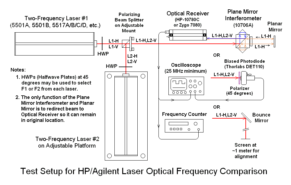
Sam S Laser Faq Laser Instruments And Applications
Frequency Counter Block Diagram Circuit Types And Its Applications
Frequency Counter Block Diagram Circuit Types And Its Applications
Ofqmyer9wiee7m
What Is The Difference Between A Johnson Counter And A Ring Counter Quora
Digital Frequency Meter Construction Working And Its Applications

Frequency Counter Using Arduino Arduino Circuit Diagram Frequencies

Frequency Counter Circuit Working And Applications Circuit Design Circuit Frequencies
Frequency Counter Block Diagram Circuit Types And Its Applications
Digital Frequency Meter Construction Working And Its Applications

Frequency Counter Circuit Working And Applications Frequencies Counter Circuit
What Are The Application Of Counters In Digital Logic Quora

Is42s16400j 7tl Memory Cad Models Datasheet Features Video Faq

Digital Frequency Meter Construction Working And Its Applications

Frequency Counter Circuit Diagram Tradeoficcom Electronic Schematics Circuit Diagram Electronics Circuit
Infrared Ir Sensor Circuit Detector Circuit Diagram Using 555 Ic
Selective Timer Alarm